Electromigration-resistant under-bump metallization of nickel-iron alloys for sn-rich solder bumps of pb-free flip-chip applications

a technology of under-bump metallization and nickel-iron alloys, which is applied in the direction of electrical apparatus, semiconductor devices, semiconductor/solid-state device details, etc., can solve the problems of not addressing the need to enhance electromigration performance, and achieve the effects of enhancing electromigration performance, eliminating or reducing electromigration, and enhancing electromigration performan

Inactive Publication Date: 2011-06-30
GLOBALFOUNDRIES INC
View PDF30 Cites 42 Cited by
  • Summary
  • Abstract
  • Description
  • Claims
  • Application Information

AI Technical Summary

Benefits of technology

The present invention offers new solutions to improve the resistance against electromigration (a metal migration caused by electric current) when designing materials for use in electronic devices like servers. This technology involves improving the properties of nitrogen iron alloy compositions which are commonly used in semiconductor packaging. By enhancing their ability to resist electromigration, this innovation can help increase the reliability and durability of components made from these materials.

Problems solved by technology

This patent discusses various challenges related to lead-free solder technologies used in electronic devices. One problem highlighted is the occurrence of white bumps during chip joining caused by cracks or delamination in the package. Another challenge is ensuring reliable connections through flip-chip joints despite the use of low-aggression solders like zinc-containing ones. Additionally, there is concern about controlling the microstructure of tin-rich solders to enhance their mechanical and electrical properties. Lastly, improving the interaction between copper surfaces and tin-rich solders remains a challenge to ensure long-term stability and prevention of failure modes associated with electromigration.

Method used

View more

Image

Smart Image Click on the blue labels to locate them in the text.
Viewing Examples
Smart Image
  • Electromigration-resistant under-bump metallization of nickel-iron alloys for sn-rich solder bumps of pb-free flip-chip applications
  • Electromigration-resistant under-bump metallization of nickel-iron alloys for sn-rich solder bumps of pb-free flip-chip applications
  • Electromigration-resistant under-bump metallization of nickel-iron alloys for sn-rich solder bumps of pb-free flip-chip applications

Examples

Experimental program
Comparison scheme
Effect test

Embodiment Construction

[0019]To achieve these and other advantages, and in accordance with the purpose of this invention as embodied and broadly described herein, the following detailed embodiments comprise disclosed examples that can be embodied in various forms.

[0020]The specific processes, compounds, compositions, and structural details set out herein not only comprise a basis for the claims and a basis for teaching one skilled in the art to employ the present invention in any novel and useful way, but also provide a description of how to make and use this invention.

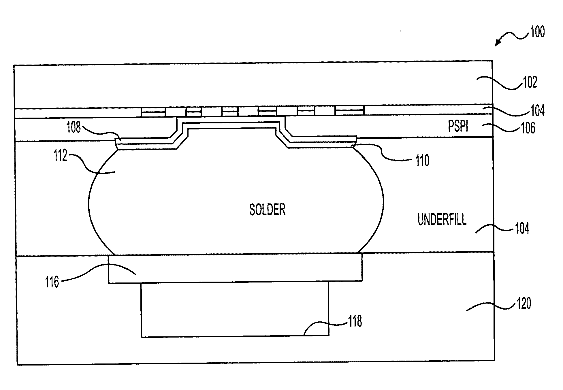
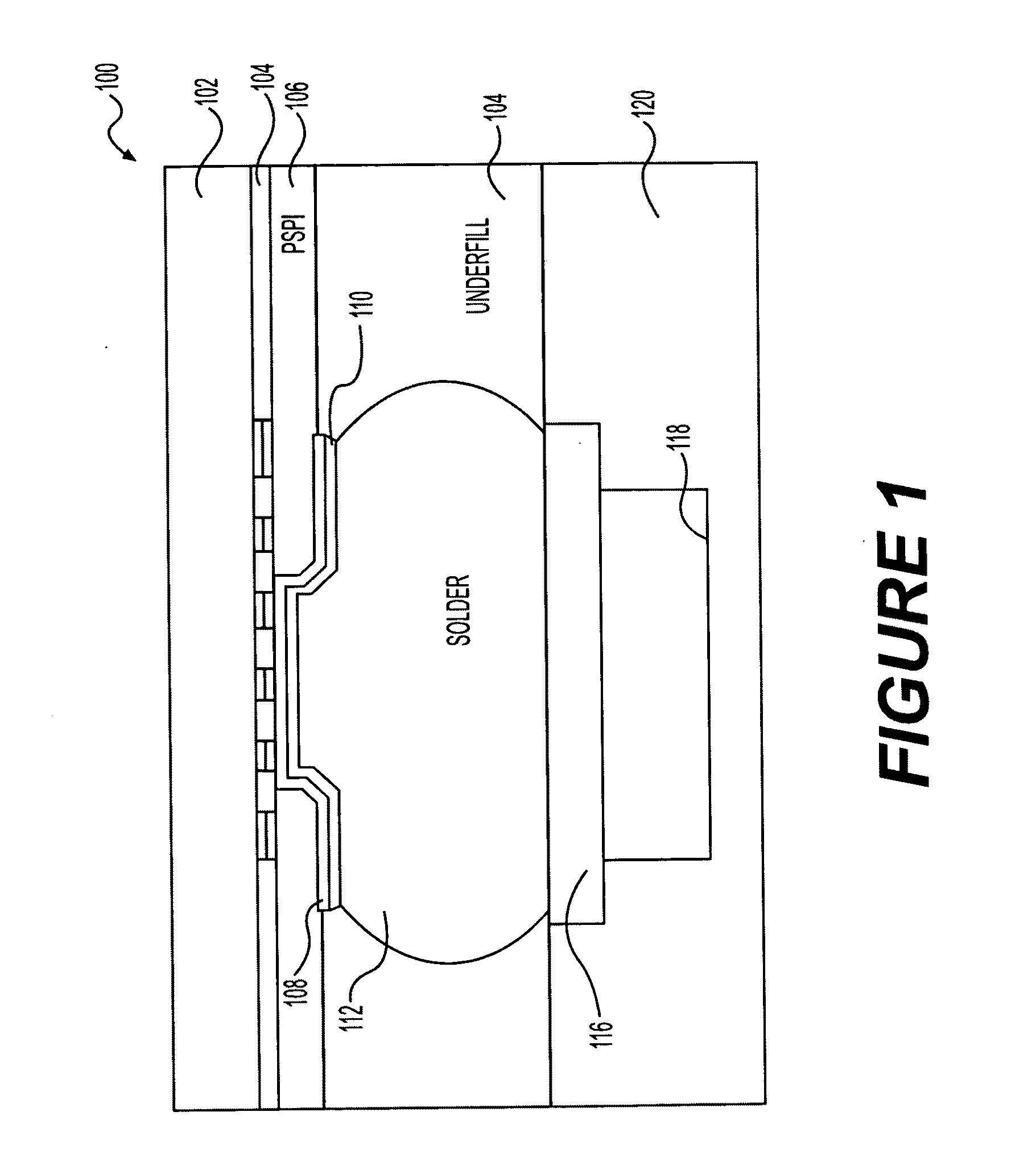
[0021]The invention comprises a process for manufacturing an electromigration-resistant under-bump metallization (UBM) flip chip structure comprising a Cu layer. This comprises applying to the Cu layer a metallic reaction barrier layer comprising Ni and Fe, where the UBM structure comprises a Sn-rich Pb-free solder bump flip chip structure. Pb-free solders for the purpose of the present invention comprise solders that are substantially free...

Login to view more

PUM

No PUM Login to view more

Abstract

A process comprises manufacturing an electromigration-resistant under-bump metallization (UBM) flip chip structure comprising a Cu layer by applying to the Cu layer a metallic reaction barrier layer comprising NiFe. The solder employed in the flip chip structure comprise substantially lead-free tin. A structure comprises a product produced by this process. In another embodiment a process comprises manufacturing an electromigration-resistant UBM Sn-rich Pb-free solder bump flip chip structure wherein the electromigration-resistant UBM structure comprises a four-layer structure, or a three-layer structure, wherein the four layer structure is formed by providing 1) an adhesion layer, 2) a Cu seed layer for plating, 3) a reaction barrier layer, and 4) a wettable layer for joining to the solder, and the three-layer structure is formed by providing 1) an adhesion layer, 2) a reaction barrier layer, and 3) a wettable layer. In a further embodiment, the reaction barrier layer comprises metals selected from Ni, Fe, Pd, Pt, Co, Cu and their alloys, and combinations thereof. A structure comprises a product produced by the immediately foregoing process.

Description

Login to view more

Claims

Login to view more

Application Information

Patent Timeline
no application Login to view more
Owner GLOBALFOUNDRIES INC
Who we serve
  • R&D Engineer
  • R&D Manager
  • IP Professional
Why Eureka
  • Industry Leading Data Capabilities
  • Powerful AI technology
  • Patent DNA Extraction
Social media
Try Eureka
PatSnap group products